 CN
CN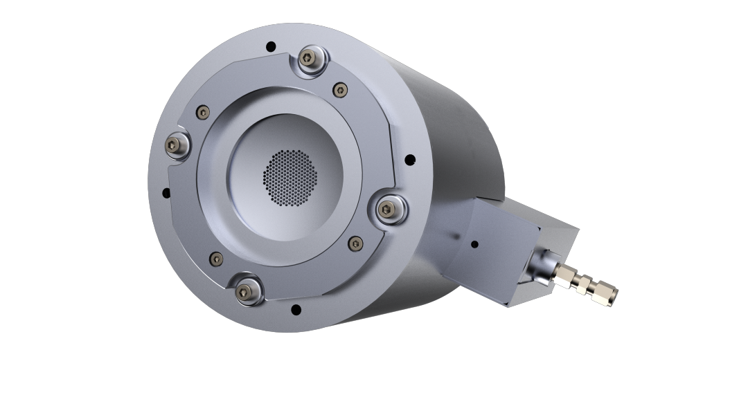
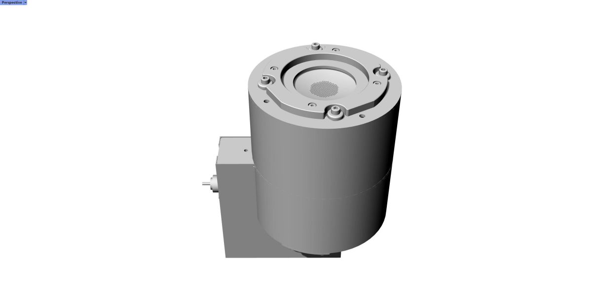
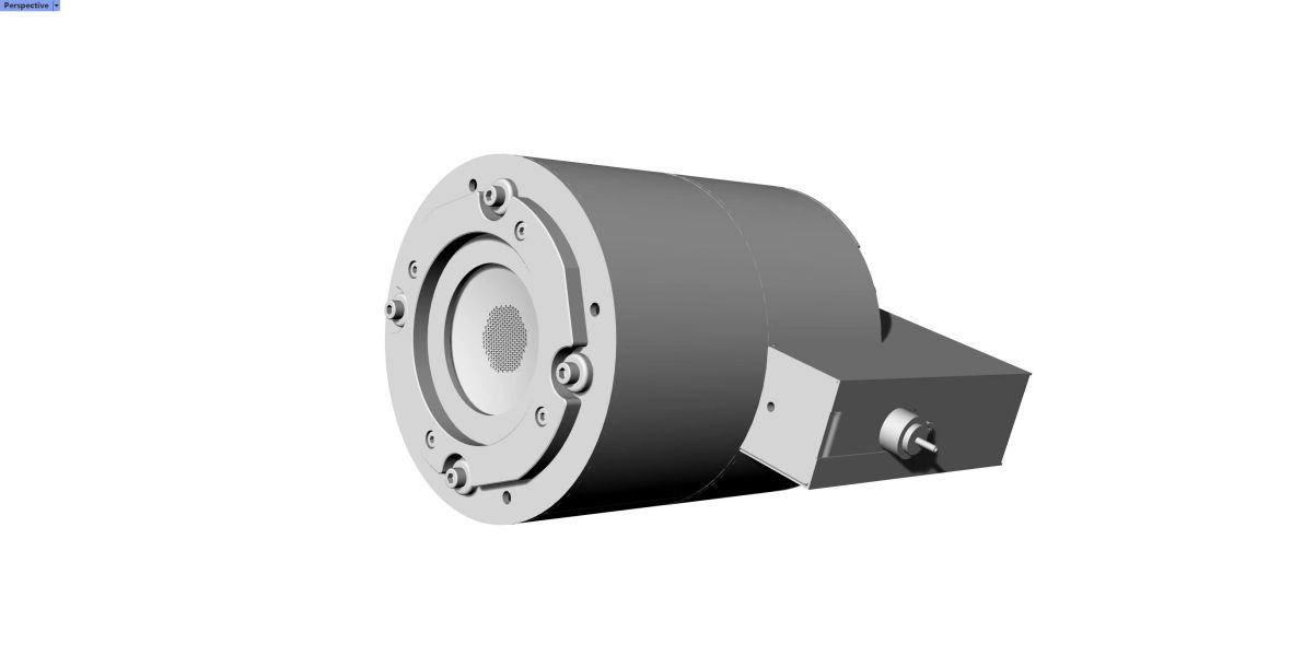
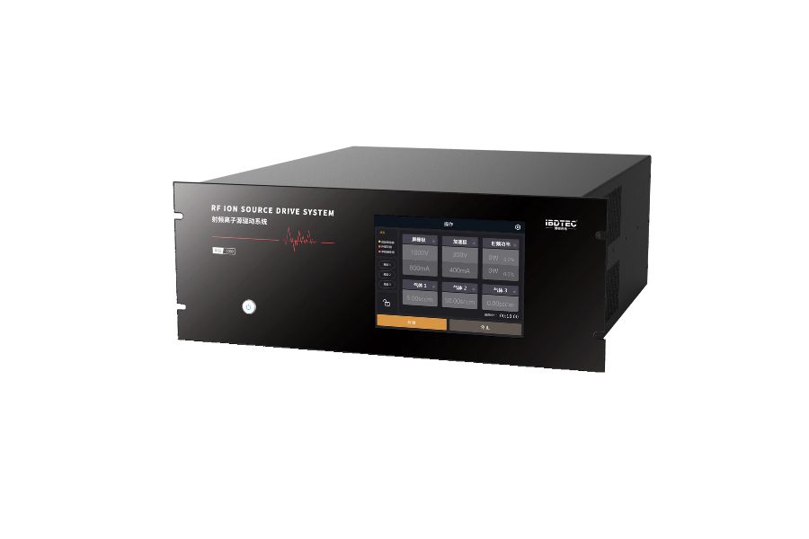
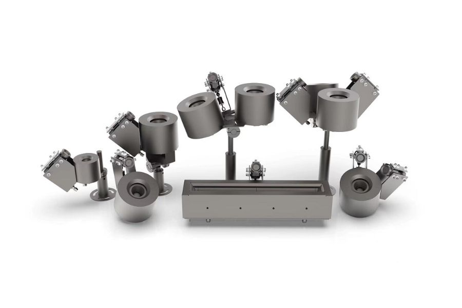
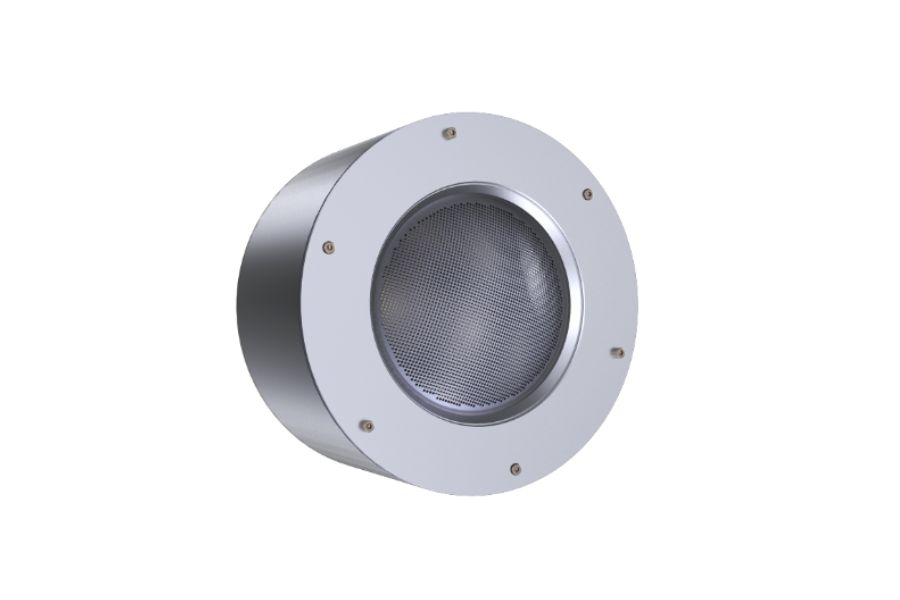
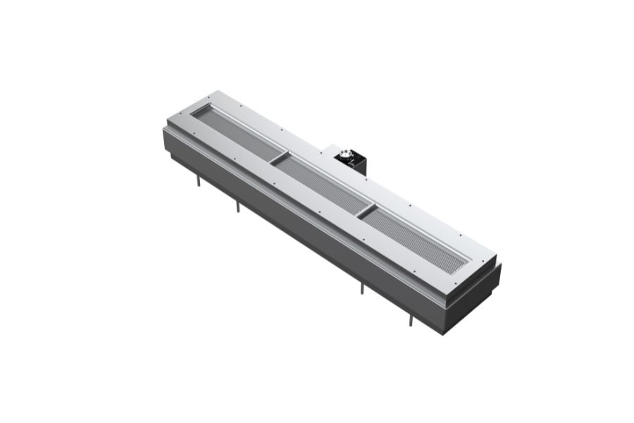
IBDTEC Tianxuan DISE series
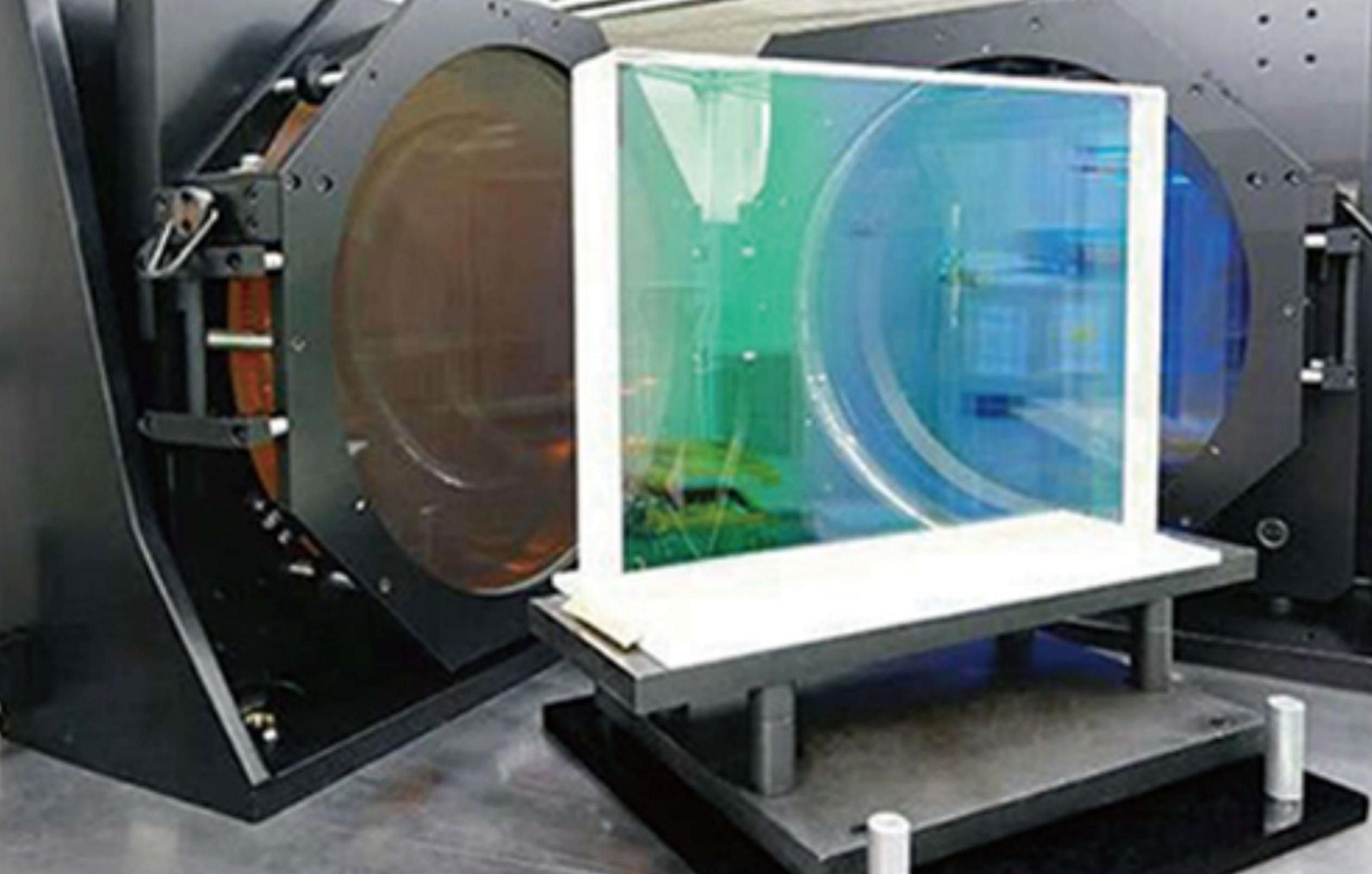
Focused DC ion source
Direction of application:
Ion beam shaping and polishing
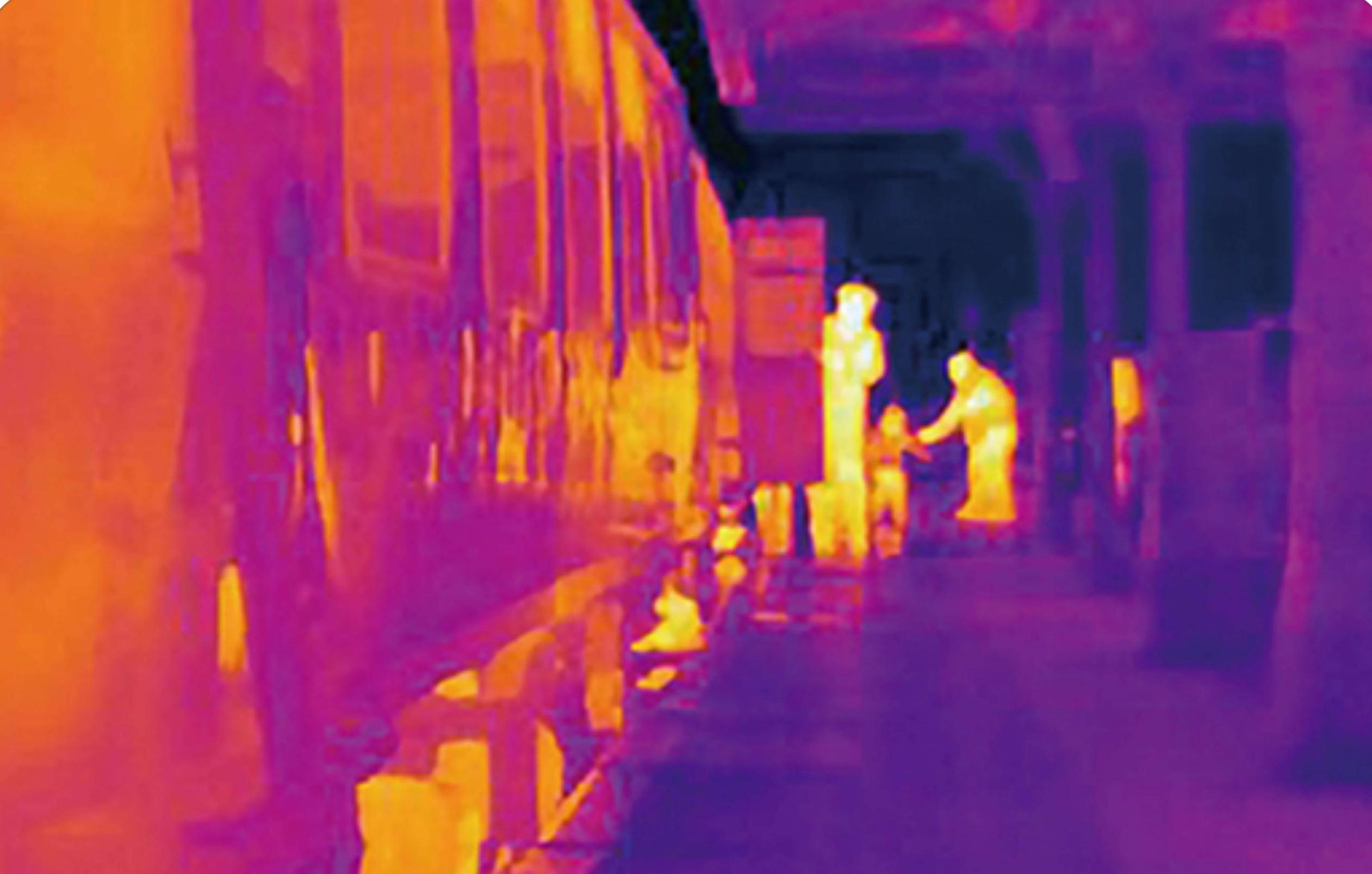
Ion beam cleaning
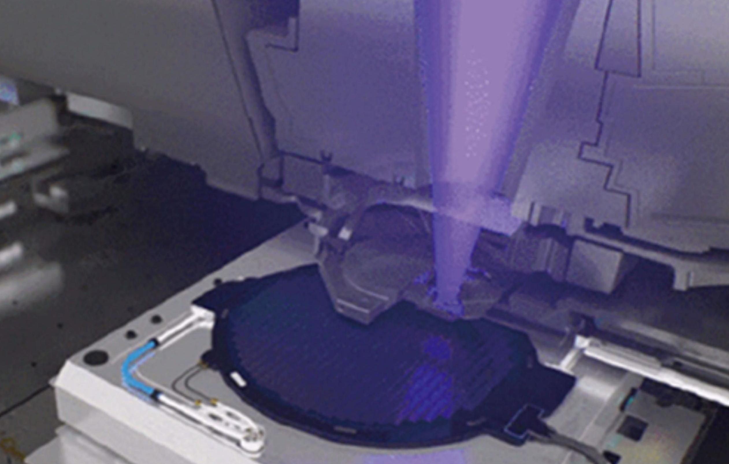
Ion beam etching
Ion beam sputtering

Product features
-
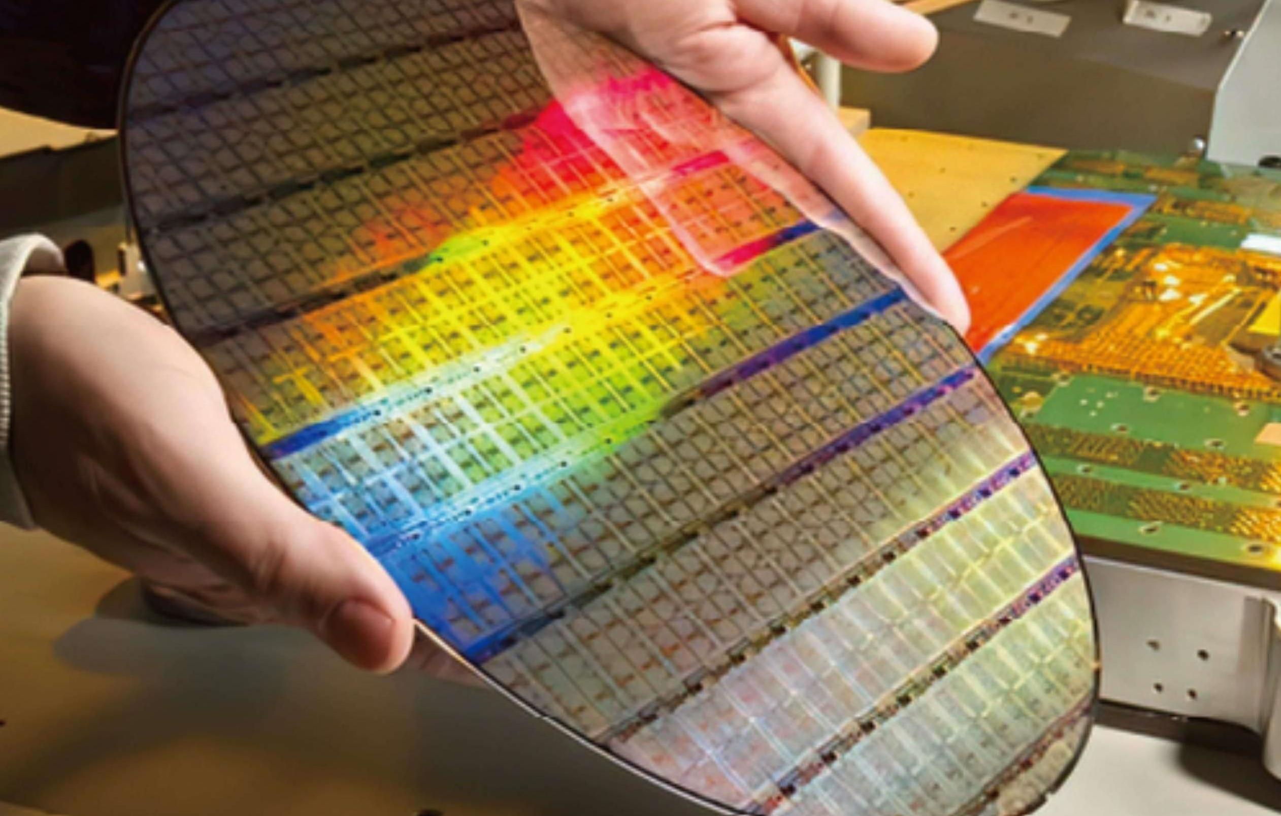
Sub-nanometer surface modification
01
-
High energy
02
-
High reliability
03
-
No filament/less pollution
04
-
Low operating costs
05
-
Support for movable structures
06
Product advantages
-
Non-contact sub-nanometer level polishing and repair
Full process normal tracking, precise removal, faster surface convergence
High precision surface correction, RMS up to 1/200 λ
Capable of achieving high-precision polishing capability with surface RMS<3nm
-
Three- or five-axis control system
The shapes of processed optical components include: flat, spherical, aspherical, freeform surface, off-axis aspherical, etc.
Angle compensation function
The materials used for processing optical components include quartz glass, microcrystals, ultra-low expansion glass (ULE), KDP crystals, sapphire, silicon, silicon carbide, infrared materials, etc.
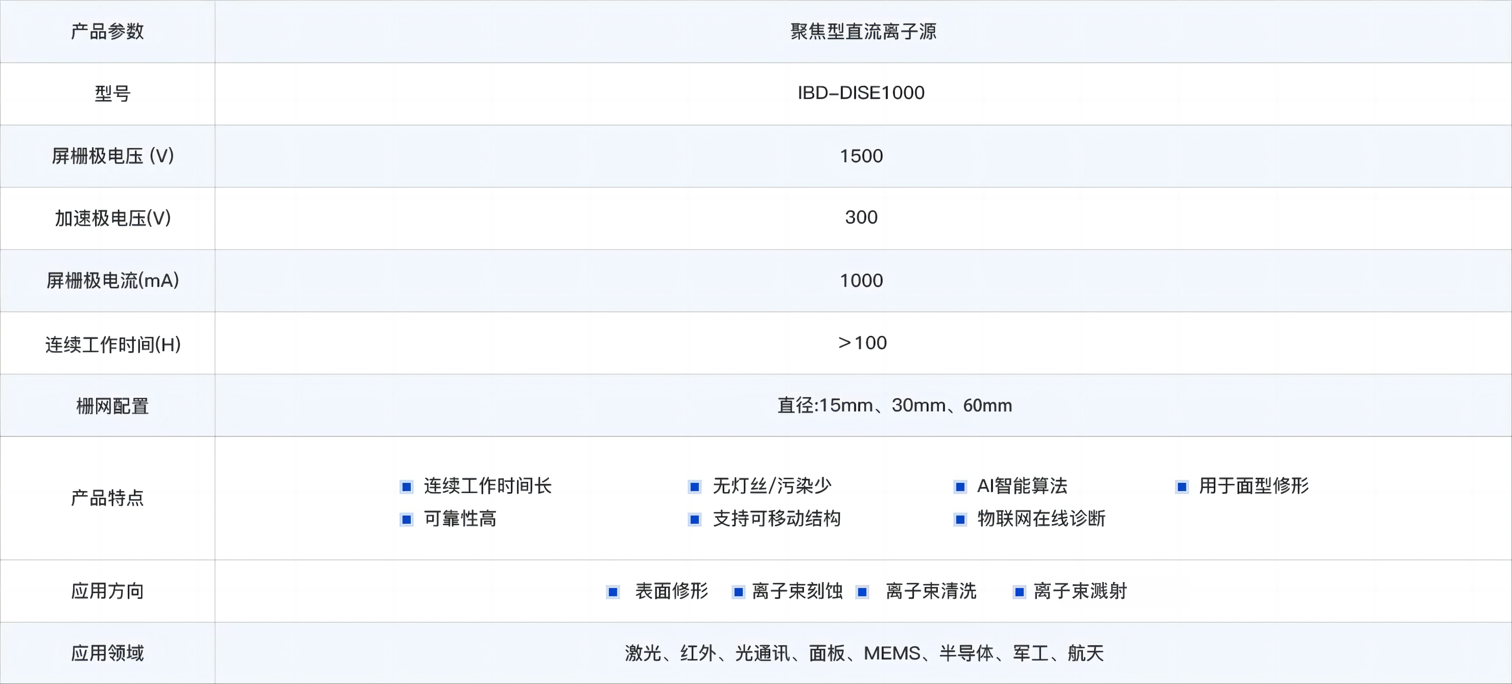
technical parameter


 Please scan code to follow us
